We support manufacturers in the selection, distribution and conversion of technical adhesives and tapes, adapted to production, assembly and performance constraints.

Recognised 3M Preferred Converter, ADDEV Materials complies with the highest 3M standards in transformation, quality and industrial reliability.

The status tesa Platinum Converter distinguishes ADDEV Materials as a strategic partner, expert in conversion, technical advice and industrial integration.

Nitto Gold Channel Partner, ADDEV Materials is renowned for its technical expertisehis process control and its ability to deliver reliable solutions.

ADDEV Materials supports industry and electronics players by offering much more than just products.
Our approach combines technical distribution, materials expertise and customised converting capabilities, to provide reliable solutions ready to be integrated into your industrial processes.
We act as a long-term technical partner, We're here to help you secure your supplies, optimise your applications and improve the overall performance of your operations.
Our adhesives and technical tapes are used in many demanding industrial environments.
We support our customers in the l'industryand consumer goodsthe POS and signageand special vehiclesthe construction and theelectronics, by offering solutions that are reliable, compliant and adapted to the constraints of use, production and sustainability.
We distribute a wide range of adhesive solutions selected from manufacturers renowned for their consistent quality and industrial performance.
These solutions address key functions such as assembly, sealing, protection, masking, electrical insulation and component encapsulation.
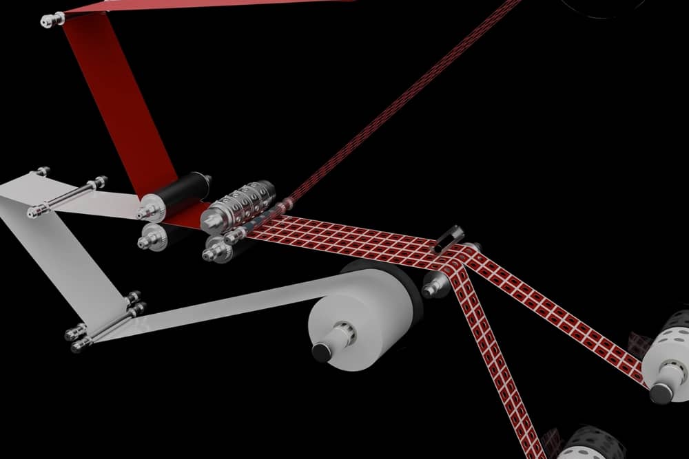
In addition to distribution, our added value lies in our ability to transform materials to adapt them precisely to your industrial uses.


Our support is not limited to products. We offer services designed to make your projects more reliable and secure your operations over the long term.

Technical support and materials expertise

Testing and prototyping

Multi-site management and secure supplies

Traceability and quality control

Digital customer portal
Our approach is based on operational efficiency, with a sustainable vision of your industrial projects.
We work with leading manufacturers of technical tapes and adhesives to guarantee the reliability, consistent quality and performance of our industrial solutions.


Deployed at most of our sites, it guarantees customer satisfaction, process performance and continuous improvement.

Specific to environmental management, it attests to our commitment to responsible, sustainable production.

International reference standard for the automotive industry, focusing on fault prevention and continuous optimisation
Are you looking for a partner capable of distributing, converting and securing your industrial adhesives and tapes?
Our teams are on hand to analyse your needs and offer you a tailored solution.

No. ADDEV Materials combines distribution of technical materials and expertise in industrial converting.
We select adhesives and tapes from benchmark manufacturers, then supply them to our customers. tailor-made transformations (functionalisation, cutting, adapted formats) for direct integration into your industrial processes.
Yes. The majority of our projects are adapted to our customers' technical constraints materials, speeds, conditions of use, standards or specific environments.
Our technical teams will work with you to define the most appropriate solution, from the material to the final format delivered ready for use.
We operate in a wide range of industrial markets, including :
general industry, consumer goods, POP & signage, special vehicles, construction and electronics.
This diversity enables us to capitalise on concrete feedback and propose tried and tested solutions.
Yes. ADDEV Materials is organised to support multi-site customers, with high requirements in terms of quality, traceability and continuity of supply.
Our industrial capacity and logistics organisation enable us to secure your flows, even for large volumes.
Absolutely. We are involved from the earliest stages in :
analyse your technical constraints,
achieve tests or prototypes,
validate the solution before industrialisation.
This approach reduces risks, costs and production times.
All you have to do is contact our experts.
After an initial discussion, we analyse your needs and guide you towards the most appropriate solution, whether it involves product selection, custom converting or optimising your existing process.